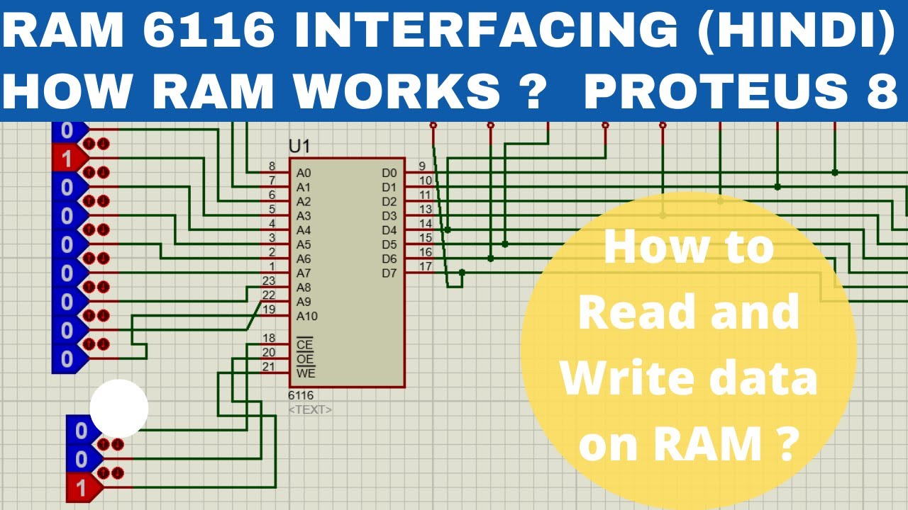
Circuit dip switch ram above j1 set chip Circuit diagram for mrram with 1k memory units. How to repair ram circuit problems-english subtitles
Watson
Binary consider Ram josh circuit zombie Ram memory cell binary watson read write circuits input access random bc line output figure select latech edu
Ram memory circuit bit cell binary circuits watson figure latech edu
Computer ram circuit diagramRam (random access memory) structure Placa de circuito do ram, pwb ilustração stockS100 computers.
Ram sap schematic memory access processor architecture randomDynamic ram 8-bit cpu – ram « benningtons.netOne bit memory circuit.
![[DIAGRAM] Logic Diagram Of Ram - MYDIAGRAM.ONLINE](https://i2.wp.com/www.researchgate.net/profile/Nasir_Ahmad7/publication/257601406/figure/fig4/AS:392541871591448@1470600683750/Block-Diagram-of-RAM.ppm)
2-bit ram circuit – downrg
Ram circuit diagramRam dimm circuit diagram Random access memory (ram) — sap-1 processor architecture documentationEce4760 final project.
3. (20 points) consider the circuit diagram for theFor the ram circuit above: a)set the dip switch j1 to Ram memory structure access random memoriesCircuit diagram of the proposed ram cell.
Ram dynamic circuit simulator electronics simulation
Ram bit cpu chips using basic benningtons bits each bytes twoRam circuit bit way value cs61c berkeley inst eecs edu processor Ram circuit diagram pdf18新利最新登入ram如何工作| howstuffworks.
Ram memory structure random access basic write ppt read powerpoint presentation select logic chip data lines addressRam block diagram Lab 4: cpu, part i: manual executionSchematic diagram of 1t rtd-based ram..

Ram ddr3 operation representation
The mystery of the zombie ram[diagram] logic diagram of ram Ddr3 pcbStatic ram circuit diagram.
Memory circuit : computer circuits :: next.grProject 3: processor design Cpu colecovision decoding resolutions techwikiCnc axis4 board schematics (rev. a).

File:colecovision-schematic---cpu,-ram,-decoding.png
Ram dimm circuit diagram .
.


For the RAM circuit above: a)Set the DIP switch J1 to | Chegg.com
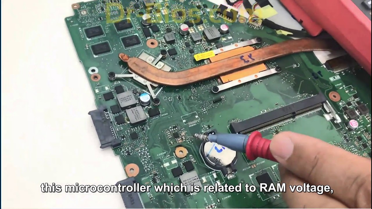
How To Repair RAM Circuit Problems-English Subtitles - YouTube

S100 Computers - 4MG RAM Card

Lab 4: CPU, Part I: Manual Execution

PCB - Ram connectors problem

Schematic diagram of 1T RTD-based RAM. | Download Scientific Diagram

3. (20 points) Consider the circuit diagram for the | Chegg.com
